[ Community Forums ] [ Products ] [ Docs ] [ Downloads ] [ History ]

| 1 |
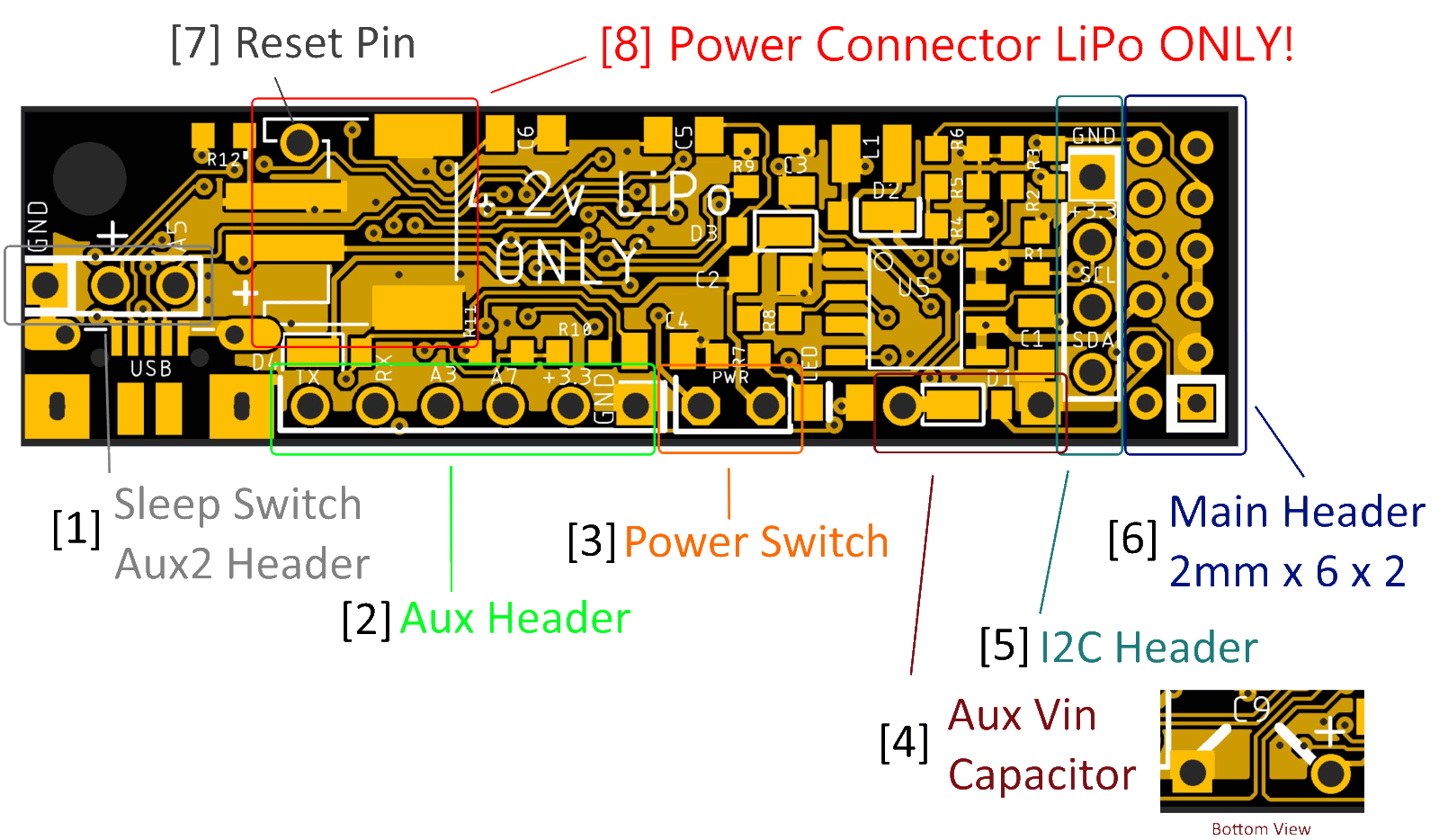
Sleep Switch: Connect a momentary switch between A5 and GND To toggle the board on/off
+3.3 switched, so safe to use with external
peripherals to turn them off. Up to 500mAh total can be drawn from all
switch +3.3v sources. Controlled with pin PA01 (active LOW)
|
| 2 |
Tx pin PA18 Rx pin PA19 A3 pin PA03 A7 pin PA07 +3.3 switched output so safe to use with external peripherals to turn them off. Up to 500mAh total can be drawn from all switch +3.3v sources. Controlled with pin PA01 (active LOW) GND |
| 3 | These two contacts come from the factory with a jumper. All power flows through here before being used by the board (except for charging, which is on its own bus). Remove the jumper and wire a switch between these two contacts for on/off support where off is off and guaranteed not to draw any power. |
| 4 | If a large capacitor is needed for voltage stability it can be wired here. These two pads are across Vin right before the switch on the PWR pads. A 4.7uF capacitor filters Vin from the factory and this has been found to be enough for most markers. |
| 5 |
The primary purpose of this header is to communicate with the OLED
board, but can be used as general IO
GND ground +3.3 switched output so safe to use with external peripherals to turn them off. Up to 500mAh total can be drawn from all switch +3.3v sources. Controlled with pin PA01 (active LOW) SCL I2C clock pin (PA08) note: A 4.7K pull-up resistor is included, and enabled with a HIGH output on pin PA11 SDA I2C data pin (PA09) note: A 4.7K pull-up resistor is included, and enabled with a HIGH output on pin PA11 |
| 6 | Main header 2mm, 2 rows of 6 pins each. This header is detailed here |
| 7 | Reset pin is located on the bottom side of the board, for those of you throwing bricks at the firmware. |